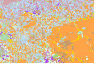
ZEISS Sigma Family
Your ZEISS SIGMA FE-SEMs for High Quality Imaging and Advanced Analytical Microscopy

ZEISS SIGMA Based on Proven Gemini Technology

• The Gemini objective lens design combines electrostatic and magnetic fields to maximize optical performance while reducing field influences at the sample to a minimum. This enables excellent imaging, even on challenging samples such as magnetic materials.

• The Gemini in-lens detection concept ensures efficient signal detection by detecting secondary (SE) and/or backscattered (BSE) electrons minimizing time-to-image.


• Gemini beam booster technology guarantees small probe sizes and high signal-to-noise ratios.

Applications

Microlens array of a CCD sensor, imaged with ETSE.

Nickel sulphide ore. Mineralogic map generated from a backscatter image and an EDS map.

Lanthanum carbonate, imaged at 1 kV at high vacuum with Inlens Duo BSE.

Ni-Cr-Fe metal spray powder coating imaged at 4 kV with HDBSD.

Accessories

smart-edx-system

SmartEDX
Discover Embedded Energy Dispersive X-ray Spectroscopy Analysis

Optimization for routine microanalysis applications and detection of low energy X-rays from light elements thanks to superior transmissivity of the silicon nitride window

Workflow-guided graphical user interface improves ease-of-use and repeatability in multi-user environments

Total service and system support by a ZEISS engineer is giving you a one-stop-shop for installation, preventive maintenance and warranty

sigma-300-rise-system

Raman Imaging and Scanning Electron Microscopy
Reap the Benefits of Fully Integrated RISE

Recognize molecular and crystallographic information

Perform 3D analysis and correlate SEM imaging, with Raman mapping and EDS data if appropriate

Fully integrated RISE lets you take advantage of both best-in-class SEM and Raman systems

Specifications